o
p
t
i
m
a
r
o
b
o
t
i
c
s

Make a Call


Make a Call
Blogs
What Are the Top 10 Dicing Machine Manufacturers?
Choosing the right Dicing Machine manufacturer requires more than comparing catalog prices. This guide examines ten leading companies serving semiconductor, electronics, medical, ceramic, and research applications. Their equipment may look similar, yet performance differs sharply under production pressure. Spindle stability, blade control, cutting accuracy, and software integration matter every day.
The comparison considers practical evidence, including cutting trials, published specifications, customer support, and long-term industry presence. A reliable machine should produce clean streets on silicon wafers, minimize chipping, and maintain accuracy across repeated batches. Cooling systems also deserve attention. Poor coolant control can affect surface quality and shorten blade life. Operators will notice these details quickly.
No single manufacturer suits every factory. A research laboratory may value flexible fixtures, while a high-volume plant may prioritize automation and cycle time. Service networks, spare-part availability, training, and installation support can influence the real cost more than the initial quotation. Claims should be checked carefully against independent records and user experience. Marketing language is not proof.
This ranking is useful, but not absolute. Regional support and application requirements can change the result. Some manufacturers offer excellent precision but limited customization. Others provide strong service while lacking advanced software. That trade-off deserves honest discussion. The following overview compares their strengths, limitations, technologies, and ideal use cases, helping buyers make a more informed decision before requesting technical proposals.
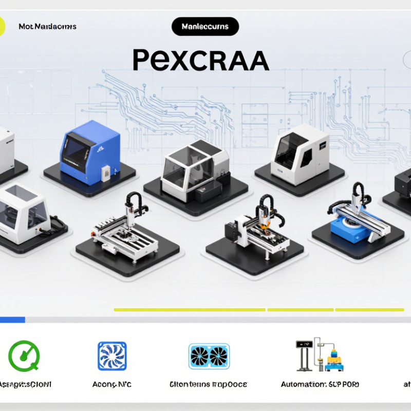
Table of Contents [Hide]
What Is a Dicing Machine and Where Is It Used?
A dicing machine cuts wafers, glass, ceramics, and other brittle materials into accurate, usable pieces. It commonly uses a diamond blade, laser, or specialized cutting wheel. In semiconductor production, the machine separates a processed wafer into individual chips. Each cut must follow narrow streets between circuits without damaging nearby components.
The equipment also serves solar-cell manufacturing, optical devices, sensors, ceramic packages, and laboratory prototypes. Operators adjust cutting speed, blade thickness, spindle rotation, cooling flow, and cutting depth. Water cooling reduces heat and carries away debris. Some systems collect particles carefully because contamination can ruin sensitive surfaces. Dust matters. Small errors matter more.
When comparing the top ten dicing machine manufacturers, buyers should examine repeatability, service support, software controls, and spare-part availability. A fast machine is not automatically the best machine. Production teams should review actual material thickness, expected throughput, acceptable edge chipping, and operator skill. In my experience, sample testing reveals problems that brochures often hide. Even a well-calibrated system may produce uneven edges when the material contains internal stress. That limitation deserves honest evaluation. Regular blade inspection, alignment checks, and cleaning routines strongly influence final quality. A machine may appear reliable during a short demonstration, yet long-term performance depends on maintenance discipline, training, and stable process conditions.
Brands
Proudly Trusted by Top Suppliers Worldwide






Let us know and we will automate, together to fit your industrial needs.
 +91-97254 16844
Clients
Proudly Trusted by Top Companies Worldwide


Do you need Help? Get in touch.
X
Please fill out the form below and we will get back to you as soon as possible.